

MAX2871 RF Board (Panelized)
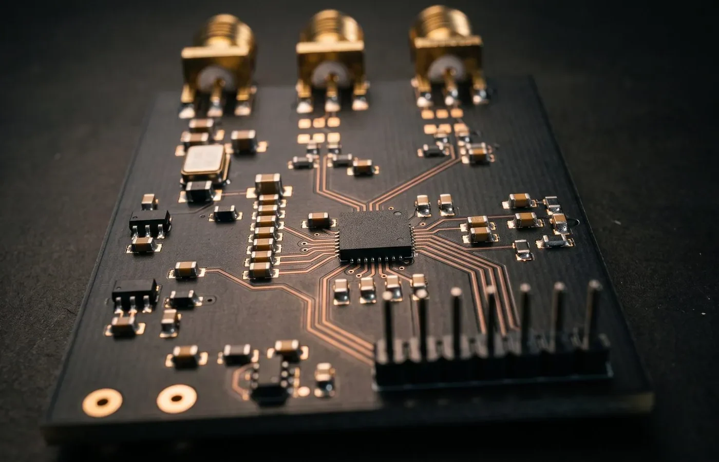
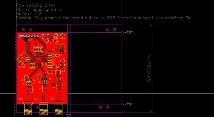
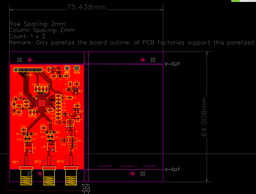
MAX2871 RF design panelized to cut unit cost for the client.
The brief
A PLL-based signal generator is dominated by the components nobody puts on the bill of materials: the reference clock’s noise, the loop filter’s stability, and the supply. The MAX2871 can reach 6 GHz; whether that output is usable is decided by how quiet everything around it is.
So the work is mostly in the reference, filtering and power rails rather than in the signal path, and the layout has to treat those three as one problem.
What we did
A compact RF signal source built around the MAX2871, a fractional-N phase-locked loop (PLL) with an integrated voltage-controlled oscillator (VCO) covering roughly 23.5 MHz to 6 GHz. It produces a tunable, low-noise RF signal for test equipment, radio and signal-generation applications, and it is configured over a simple digital interface.
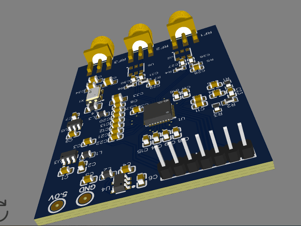
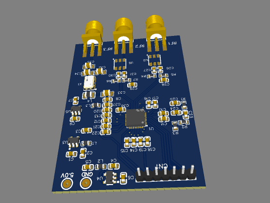
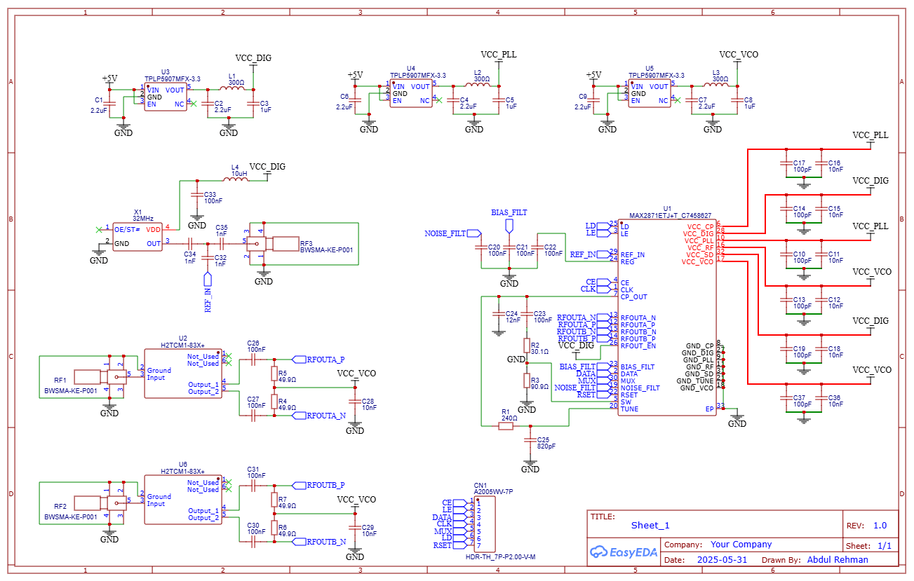
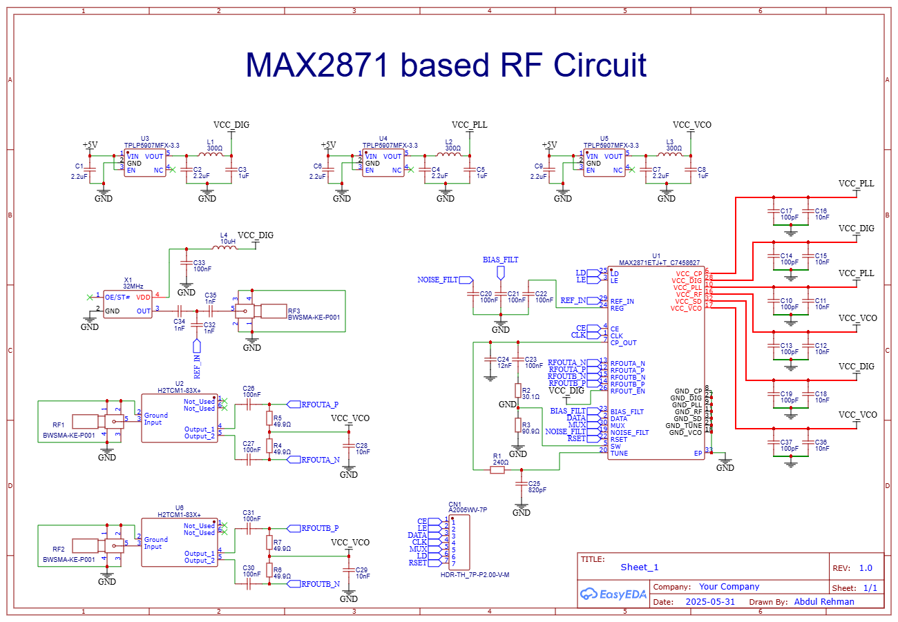
- Two RF outputs: The MAX2871’s differential outputs (RFOUT A and B) are each converted to single-ended 50 Ω by a balun (H2TCM1-83X+) and brought out to SMA connectors (RF1 and RF2). Each output has its own bias network and decoupling.
- Reference clock: A 32 MHz oscillator, filtered and AC-coupled, drives the PLL reference input. The reference is also brought out to a third SMA connector (RF3).
- Low-noise power design: Three separate TPLP5907 low-noise LDO regulators power the digital, PLL and VCO supplies independently from the 5 V input. Each has an inductor/capacitor filter, and every supply pin has 100 pF and 10 nF bypass capacitors. This is key for good phase noise.
- Loop filter: A passive loop filter on the charge-pump output sets the PLL’s tuning and lock behavior.
- Digital control: A 7-pin header exposes the control lines (chip enable, load enable, data, clock, mux out, lock detect and reset) so the chip can be programmed by a microcontroller.
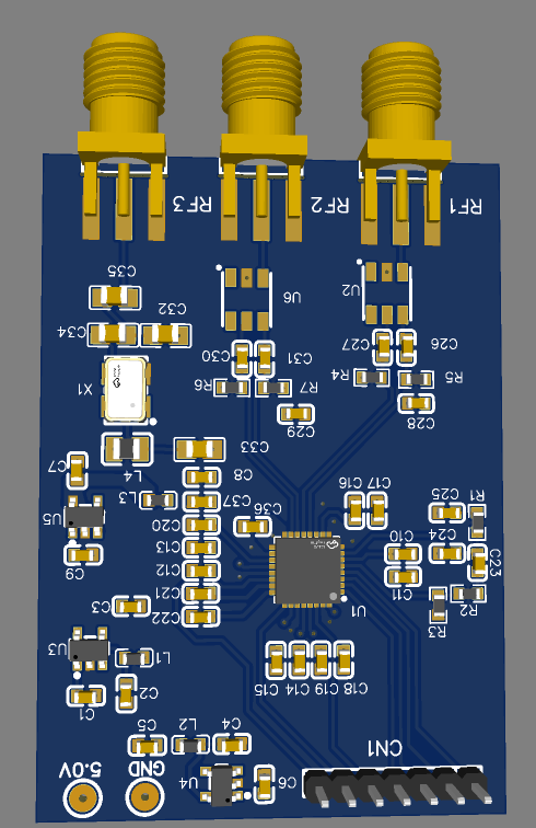
- Layout: A compact four-layer-style RF layout with a solid ground plane, the RF outputs routed to the board edge with short traces to the SMA connectors, and the analog and digital sections separated. The board is panelized with V-cuts for fabrication.
Design details
Design summary
| CAD tool | EasyEDA |
|---|---|
| Overview | A compact RF signal source built around the MAX2871, a fractional-N phase-locked loop (PLL) with an integrated voltage-controlled oscillator (VCO)… |
| Two RF outputs | The MAX2871’s differential outputs (RFOUT A and B) are each converted to single-ended 50 Ω by… |
| Reference clock | A 32 MHz oscillator, filtered and AC-coupled, drives the PLL reference input. |
| Low-noise power design | Three separate TPLP5907 low-noise LDO regulators power the digital, PLL and VCO supplies… |
| Loop filter | A passive loop filter on the charge-pump output sets the PLL’s tuning and lock behavior. |
| Digital control | A 7-pin header exposes the control lines (chip enable, load enable, data, clock, mux out, lock… |
| Layout | A compact four-layer-style RF layout with a solid ground plane, the RF outputs routed to the… |
Have a board like this?
Send us the schematic, the mechanical constraints and the deadline. We will tell you what it takes and what it costs.