
High-Speed Layout
Constraints first, copper second. We decide which nets are fast, where a signal may cross a split and where matching is genuinely required — then hold the layout to those rules and write down why.
- Stack-up before layout
- Return-path discipline
- Constraint-driven routing
What high-speed layout means here
Constraints are set before layout begins: which nets are fast, how far one may cross a split, and where matching is actually required. The layout is then held to them, and the reasons are written down so the next person who opens the project can see why a trace went where it went.
High-speed is not a style. It is a set of decisions about reference planes, return paths and length, made explicit and checked against the fabricator’s stack-up rather than against a generic rule of thumb.
What we handle
- Stack-up definition — layer order, copper weights and dielectric thicknesses chosen against the impedances your nets need and the board your fabricator can build.
- Reference planes — unbroken planes under fast edges, with splits placed where they do the least damage and documented where they cannot be avoided.
- Length matching — where it is actually required, with the tolerance set against the interface and the fabricator’s capability, not a generic number.
- Return-path continuity — stitching vias, plane changes, and the places a signal crosses a gap.
- Decoupling — placement, loop area, and the difference between a capacitor that is present and one that is effective.
- Constraint documentation — the rules the layout was held to, written into the project so they survive the next revision.
What you get back
A fabrication package: Gerbers, drill files, stack-up, fabrication notes and the constraint set the layout was run against. The same files your fabricator needs, with the reasoning attached so a future change does not quietly undo a decision.
How it runs
Send the schematic, the mechanical constraints, the target interfaces and the date the first prototype has to exist. We confirm the stack-up against your fabricator before a single trace is placed, then lay out against the agreed constraints.
Figures for differential impedance and length tolerance are industry references — confirm the real values against your fabricator’s stack-up for the material and build you have quoted.
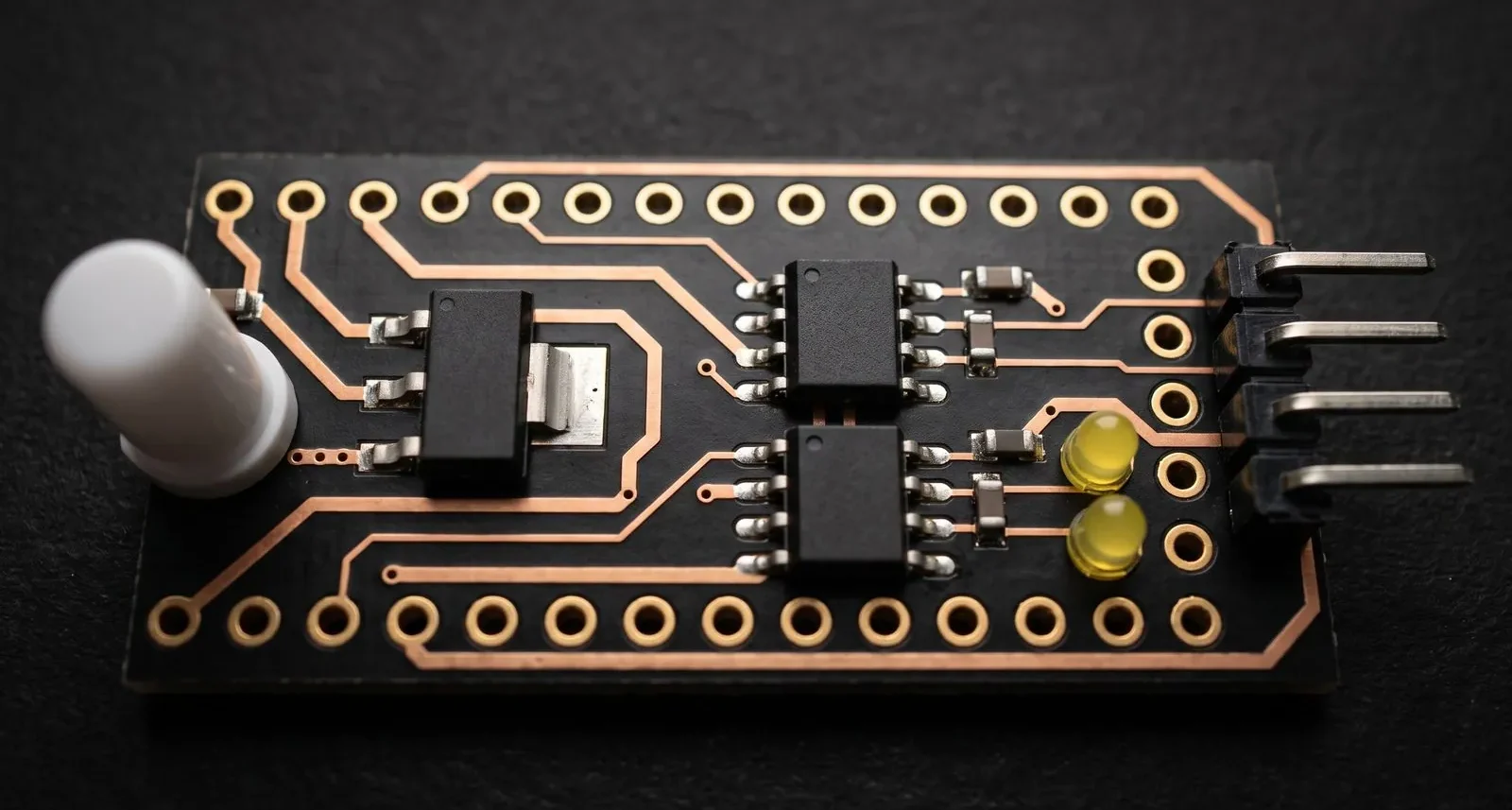
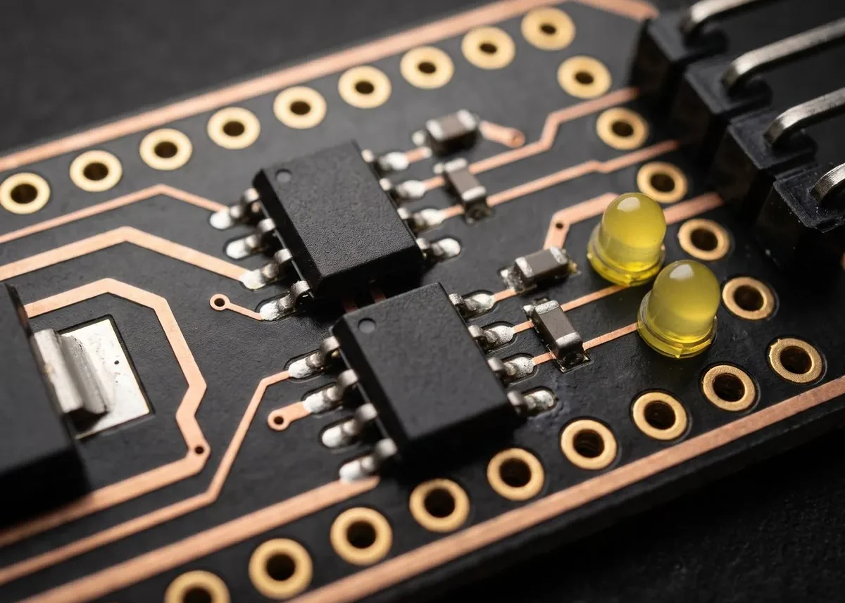
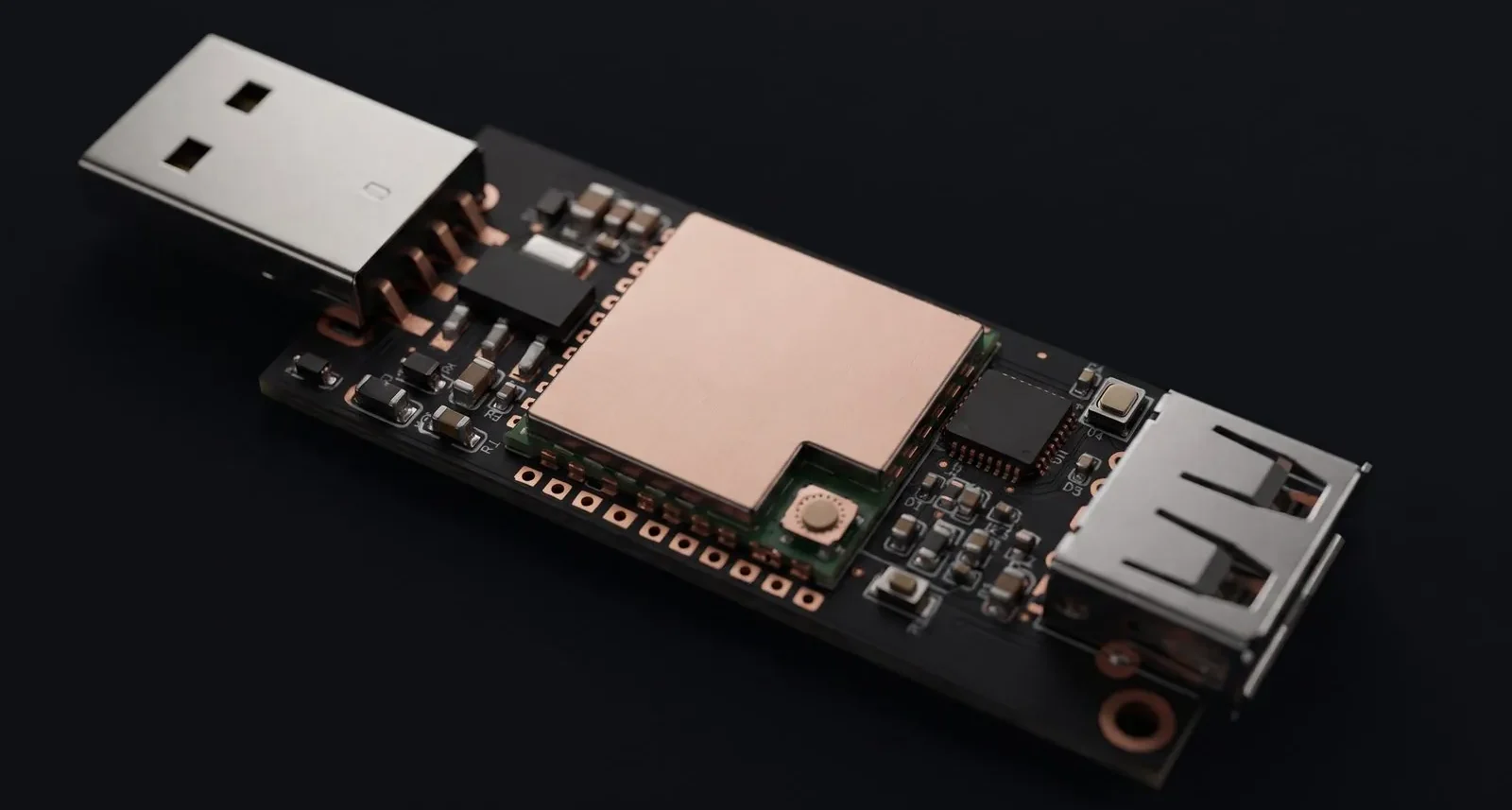
Boards that went through this.
Released hardware from the Interfaces & Hubs archive — the same discipline applied to a real board, not a sample layout.



Related practices.
-
 Altium Designer
-
 KiCad
-
 EasyEDA
-
 Cadence Allegro
Send us the schematic.
Tell us your layer limits, the critical signals and the date the first prototype has to exist. You get an honest feasibility answer and a fixed scope before any work starts.