

Schematic Review
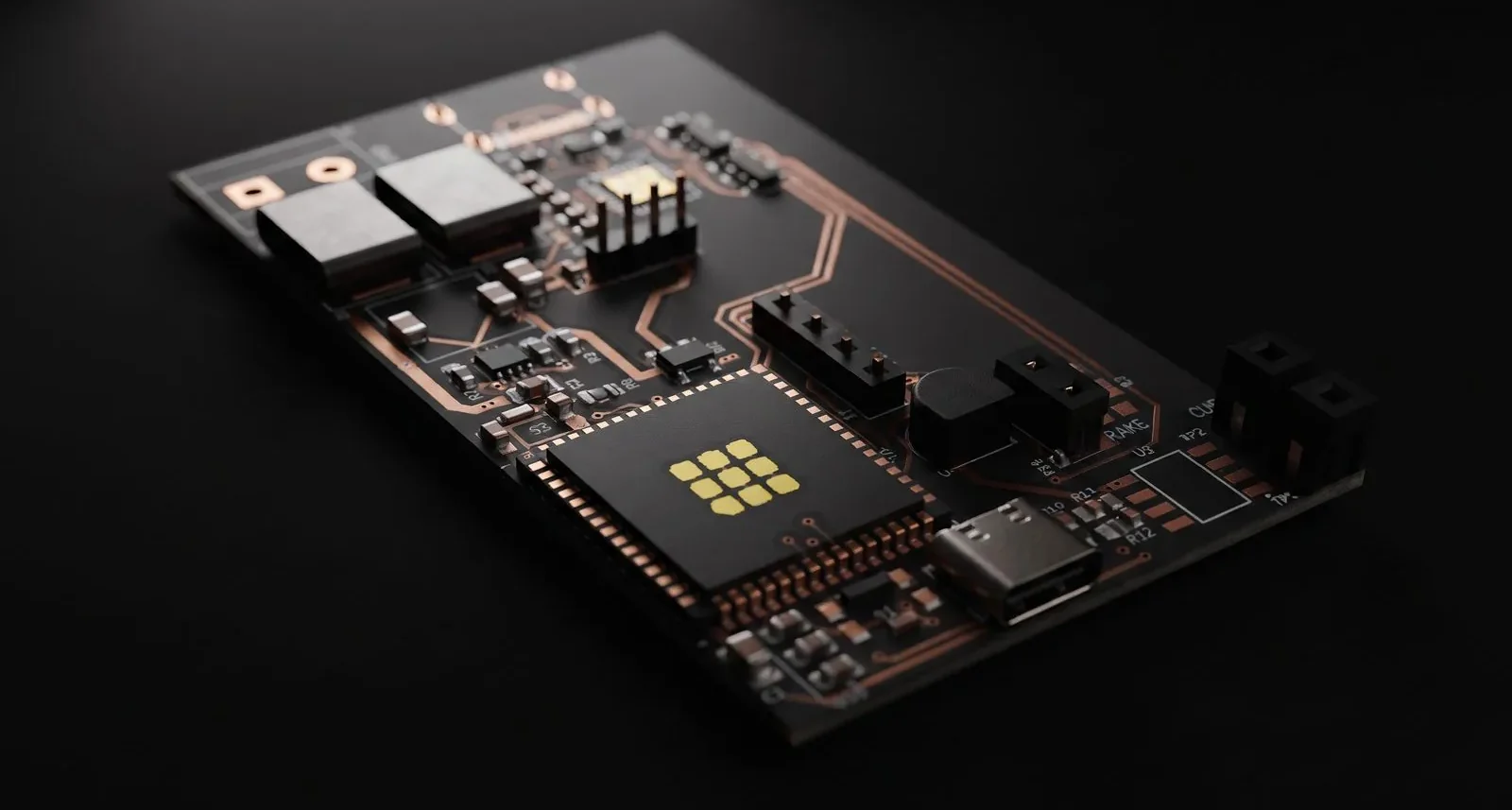
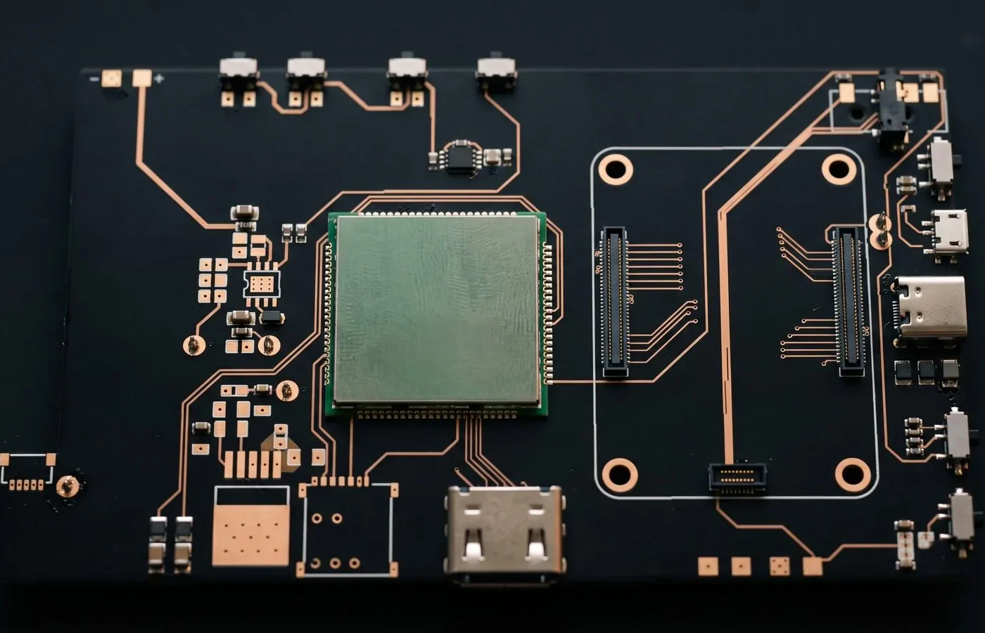
Component logic, datasheets and netlists verified before layout begins, so functional errors never reach the copper.
We take high-speed digital, mixed-signal, RF and HDI boards from schematic review to a fabrication package your manufacturer can build without a callback.
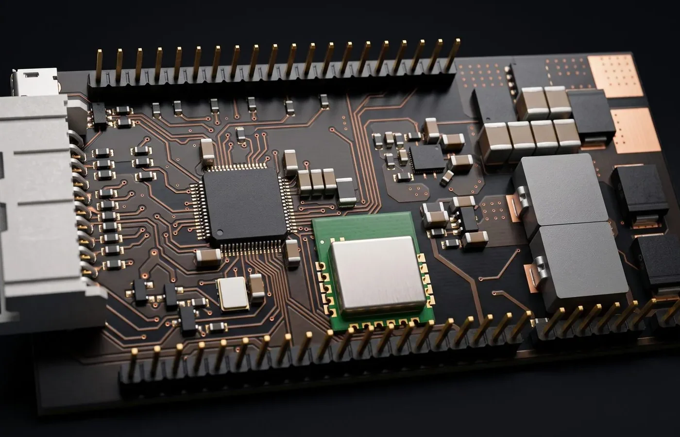
Schematic review, stack-up, layout and verification — then a release package checked against your fabricator’s own process before handoff.
Component logic, datasheets and netlists verified before layout begins, so functional errors never reach the copper.
DDR4/5, PCIe and SERDES routed with controlled impedance, length matching and a continuous return path on every net.
Reference planes, stitching vias and antenna keep-outs planned while the board is routed, not retrofitted once it fails.
Gerbers, NC drill and pick-and-place checked against your fabricator’s stated process and assembly rules before release.
We do not just connect pins. Every trace is a transmission line. Each of these four areas is a practice in its own right — see the full service list for what each one covers.
DDR4/5, PCIe and SERDES. Exacting length matching, controlled impedance and differential pair tuning.
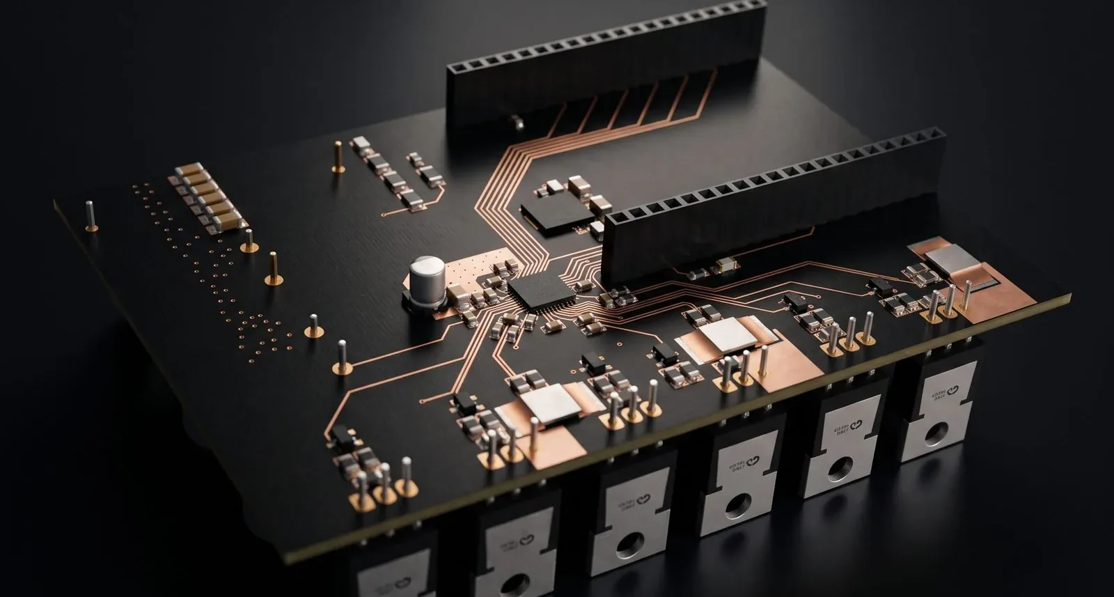
Solid-state relays and BMS. Heavy current routing and thermal management without runaway.
ESP32 integration and custom antenna matching. Isolated planes for maximum range.
Up to 16 layers. Blind, buried and micro-vias for dense packaging.
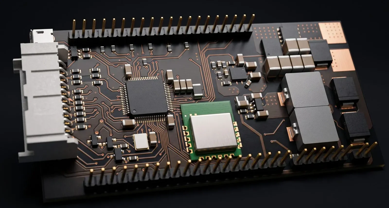
We verify component logic, datasheets and netlists before a single pad is placed.
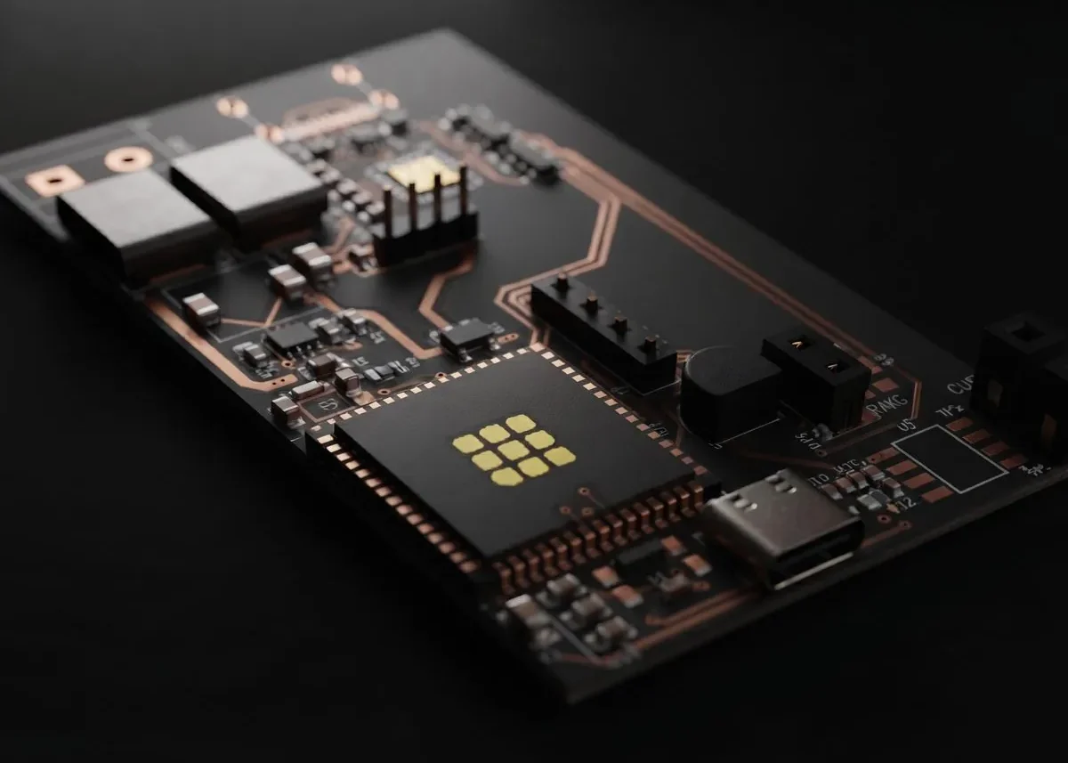
Components positioned to prioritise critical signal paths and thermal dissipation.
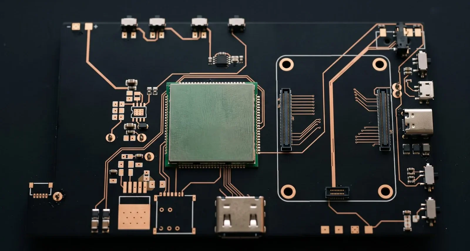
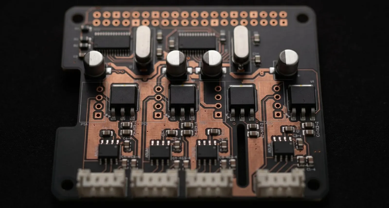
Precise copper traces with calculated impedance and strict clearance rules.
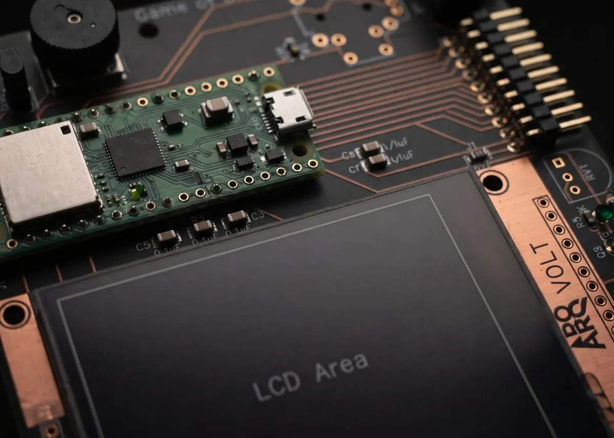
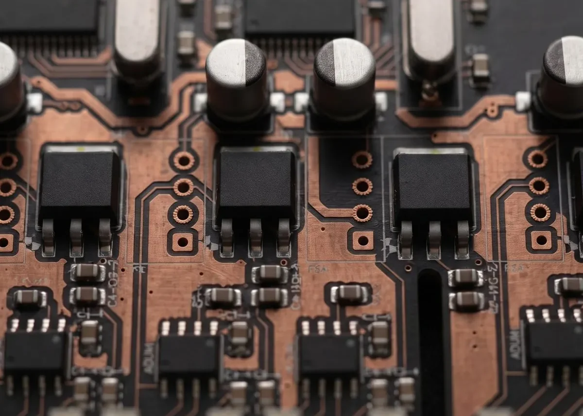
Verified Gerbers, NC drills and pick-and-place files, ready for assembly.
Thermal throttling and EMI do not exist on paper. We route against physical constraints so the board behaves the same on the bench as it did in simulation. Where a board is already failing, a design review finds the cause before anyone touches copper.
A cross-section of recent work across motor control, RF, power, industrial I/O and embedded platforms. Each board runs schematic capture, layout and verification before release, and ships with the package your fabricator needs. Filter by what the board has to do.
No projects in that category.
A good design that cannot be built is a failed design. We format every manufacturing output for turnkey assemblers, and check DFM/DFA against the fabricator's own process before release. If a package has already been rejected, that is a DFM review, not a redesign.
Based in Karachi, Pakistan. We design high-speed DDR4, PCIe and SERDES boards for semiconductor test equipment, and help hardware teams take IoT prototypes to fabrication-ready release. Every project is reviewed by the engineer who will stand behind it — more on how we work.
Scope, layer count and interface count drive the number — the reasoning is set out in our cost FAQ. A 30-minute consultation is booked separately and credited against the first milestone.
Excellent PCB design work in EasyEDA! The circuit layout was well organized, with careful component placement, accurate routing, and attention to connectivity. The design files were prepared professionally, communication was smooth, and the project was completed on time. Highly recommended!
 United Kingdom
Thank you for your help and excellent job. Highly recommended!!
 United States
Very satisfied with the PCB design service! The schematic and board layout were completed with precision, and the component footprints and connections were handled carefully. The work showed solid technical knowledge, attention to detail, and timely delivery. Would gladly work together again!
 Canada
The PCB design work was excellent! The circuit layout was carefully designed, with well-organized component placement and attention to routing and connectivity. The files were professionally prepared, communication was smooth, and the final result met the project requirements perfectly. Highly recommended!
United StatesExcellent work from Abdul again will definitely use his service again
 Australia
We deliver native source files in Altium Designer, KiCad, EasyEDA or Cadence Allegro, depending on the standard your team already uses.
We provide the design engineering. You receive the exact package needed to upload to JLCPCB, PCBWay or your local fabricator for manufacture and assembly.
Yes. Layout audits are a core service. We check trace clearances, power planes and antenna keep-outs to identify why a prototype is failing in test.
Complete design source files, production files (Gerber, NC Drill and Pick & Place), a detailed BOM with sourcing links, and 3D STEP models of the finished board for mechanical fit.
It depends on layer count, interface count and how complete your schematic is. A simple single-board prototype is typically delivered in days; high-speed multi-layer work is quoted by milestone. Send us your constraints and we will give you a timeline and budget estimate.
Yes. We work globally and in English. Roughly half our work comes through Upwork and Fiverr, with direct engineering teams commissioning projects remotely.
Tell us the layer count, the interfaces and where the board has to survive. We will come back with an architecture view, a timeline and a number.
Start a Project Browse Services