RS-485 PCB Design: Termination, Fail-Safe Biasing and Isolation
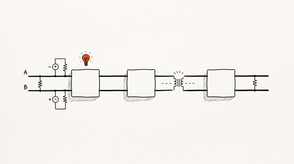
RS-485 PCB design guidance: 120 ohm termination, fail-safe biasing, the common-mode budget, galvanic isolation and the checks to run before release.
Field notes from the workbench — high-speed routing, stack-up calculation, return-path planning, and DFM lessons learned across 150+ board fabrications.
RS-485 PCB design guidance: 120 ohm termination, fail-safe biasing, the common-mode budget, galvanic isolation and the checks to run before release.
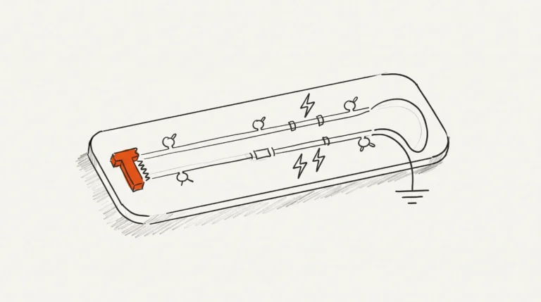
CAN bus PCB design in practice: where 120 ohm termination goes, what split termination does, where ESD protection belongs and why the ground reference is a layout decision.
USB 3.0 layout rules that matter: 90 ohm differential impedance, the 150 mil length mismatch budget, reference plane continuity and connector escape.
What an independent PCB design review checks before you spend money on boards, what it catches that a DRC pass cannot, and what to send for one.
What a PCB design actually costs, why layer count and interface speed move the number more than board size does, and how to read a quote you can trust.
Tell us the layer count, the interfaces, and where the board has to survive. We will come back with an architecture view, a timeline, and a clear budget.