
Services
Schematic review, high-speed layout, RF and return-path integrity, and DFM verification — four practices that take a board from netlist to fabrication release.
Four practices, one discipline.
Take one on its own, or run the whole path from schematic review through to fabrication release. Each practice catches what the others miss.
DFM / DFA Verification
Checked against your fabricator’s process before release
Explore serviceHigh-Speed Layout
DDR4/5, PCIe and SERDES with controlled impedance
Explore serviceSchematic Review
Component logic, datasheets and netlists verified before layout
Explore serviceSignal & Return-Path Integrity
Reference planes, stitching vias and keep-outs planned in
Explore serviceEngineering Methodology
Every layout in this practice starts directly from your netlists and component constraints rather than generic proposal forms. We model exact trace geometries with field solvers, uphold strict return path discipline, and format all outputs for turnkey fabrication.
Send your schematic files along with mechanical enclosure limits, and we will confirm the layer stackup, impedance targets, and delivery schedule before work begins.
Related hardware tape-outs.
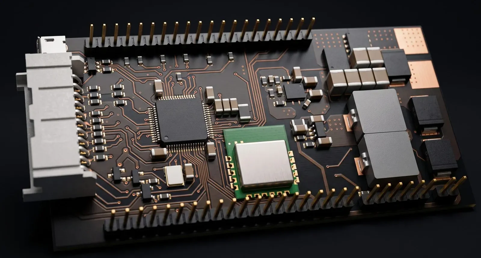
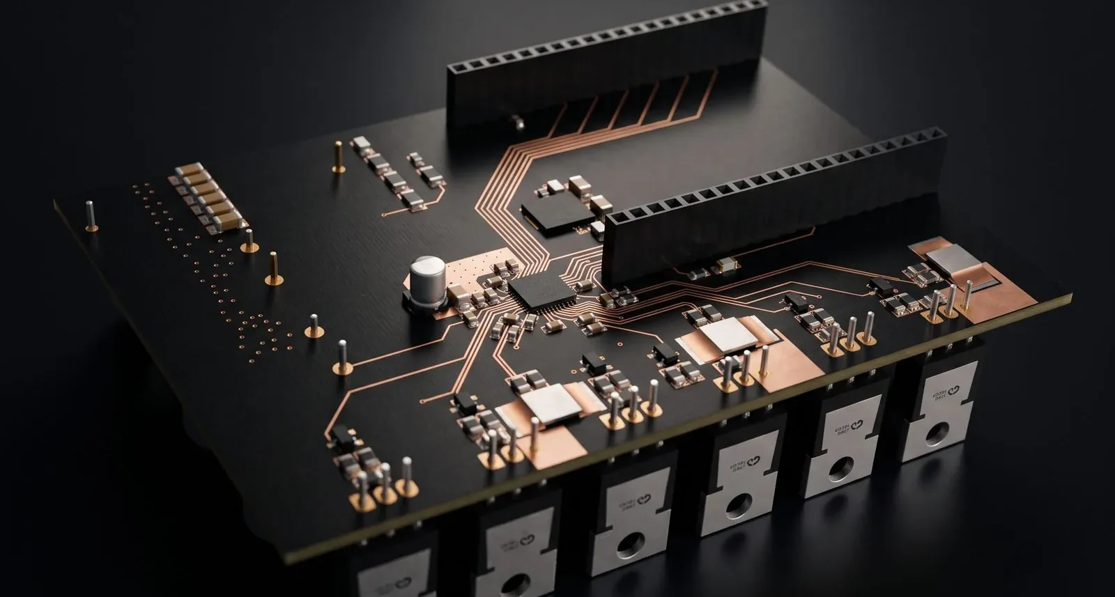
Production boards engineered through this exact discipline — verified on the bench and released with turnkey packages.



Send us the schematic.
Tell us your layer limits, critical signal paths, and fabrication targets. Abdul will personally inspect your architecture and provide an honest feasibility breakdown.