

TQP369181G RF Board
RF board with coaxial connectors and ground stitching for signal integrity.
The brief
Chaining gain stages is easy on paper and unforgiving in practice. Each stage has to be biased, DC-blocked and matched to 50 Ω, and the gain only stacks if every impedance between the connectors is actually 50 Ω.
SMA connectors at the inputs, the outputs and between every stage were the enabling decision: they turn the board into its own test instrument, so each block can be measured in isolation instead of inferred from the whole chain.

What we did
A 50 Ω RF amplifier board that chains several wideband gain stages, with SMA connectors at the inputs, outputs and between stages for measurement.
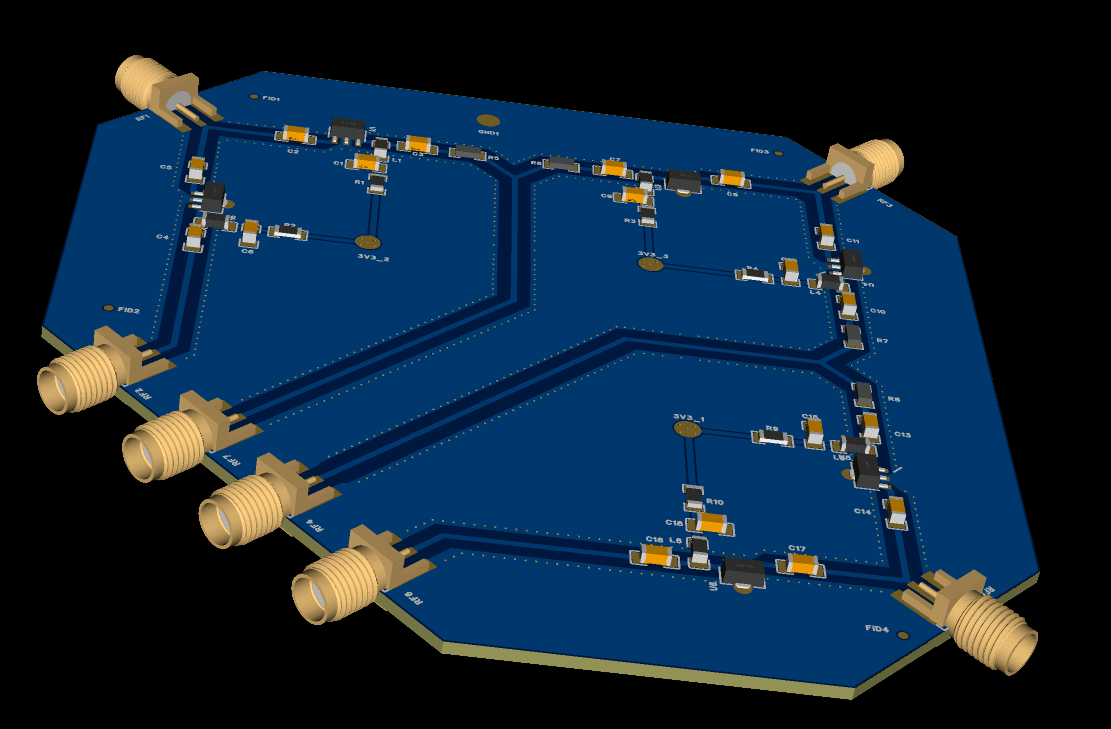
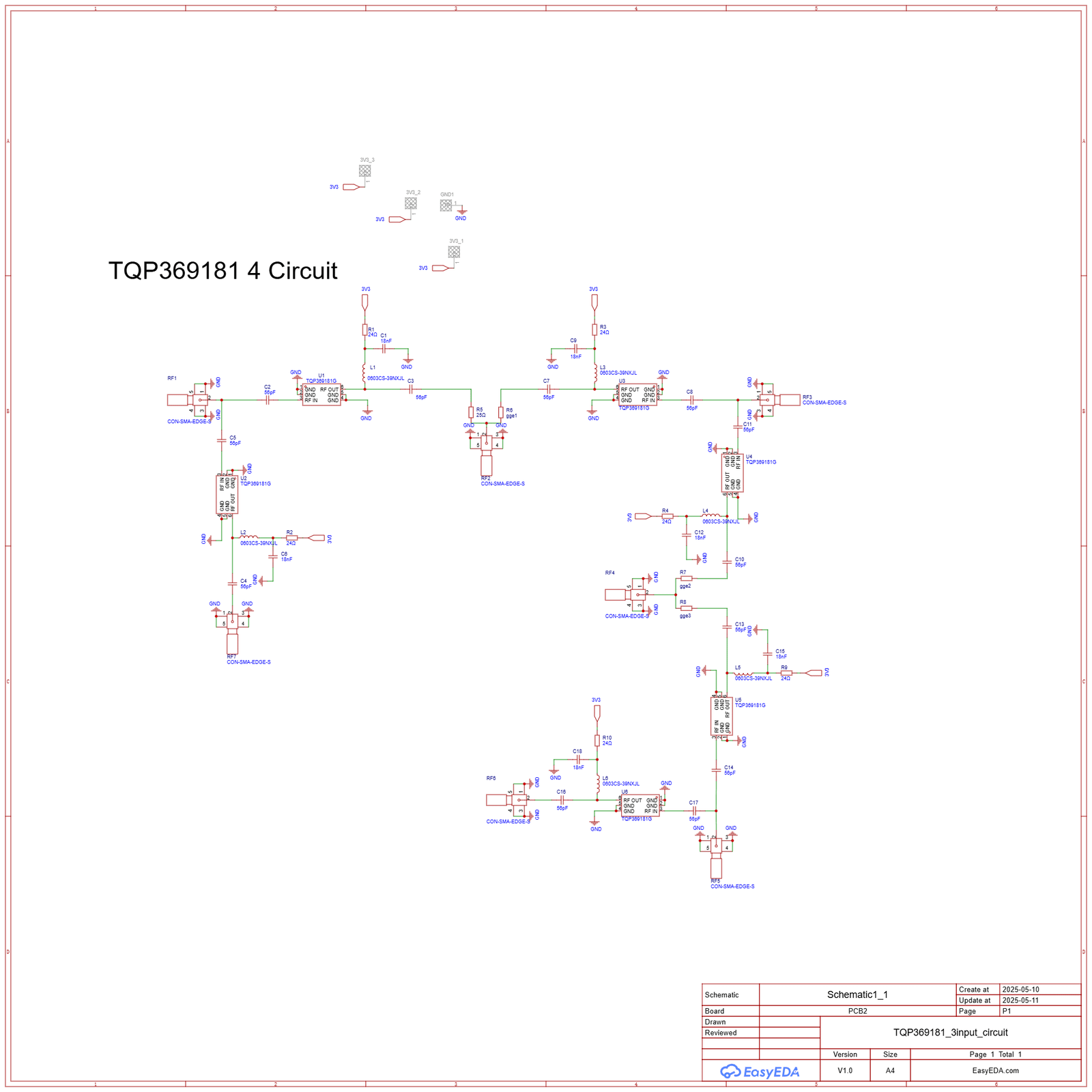
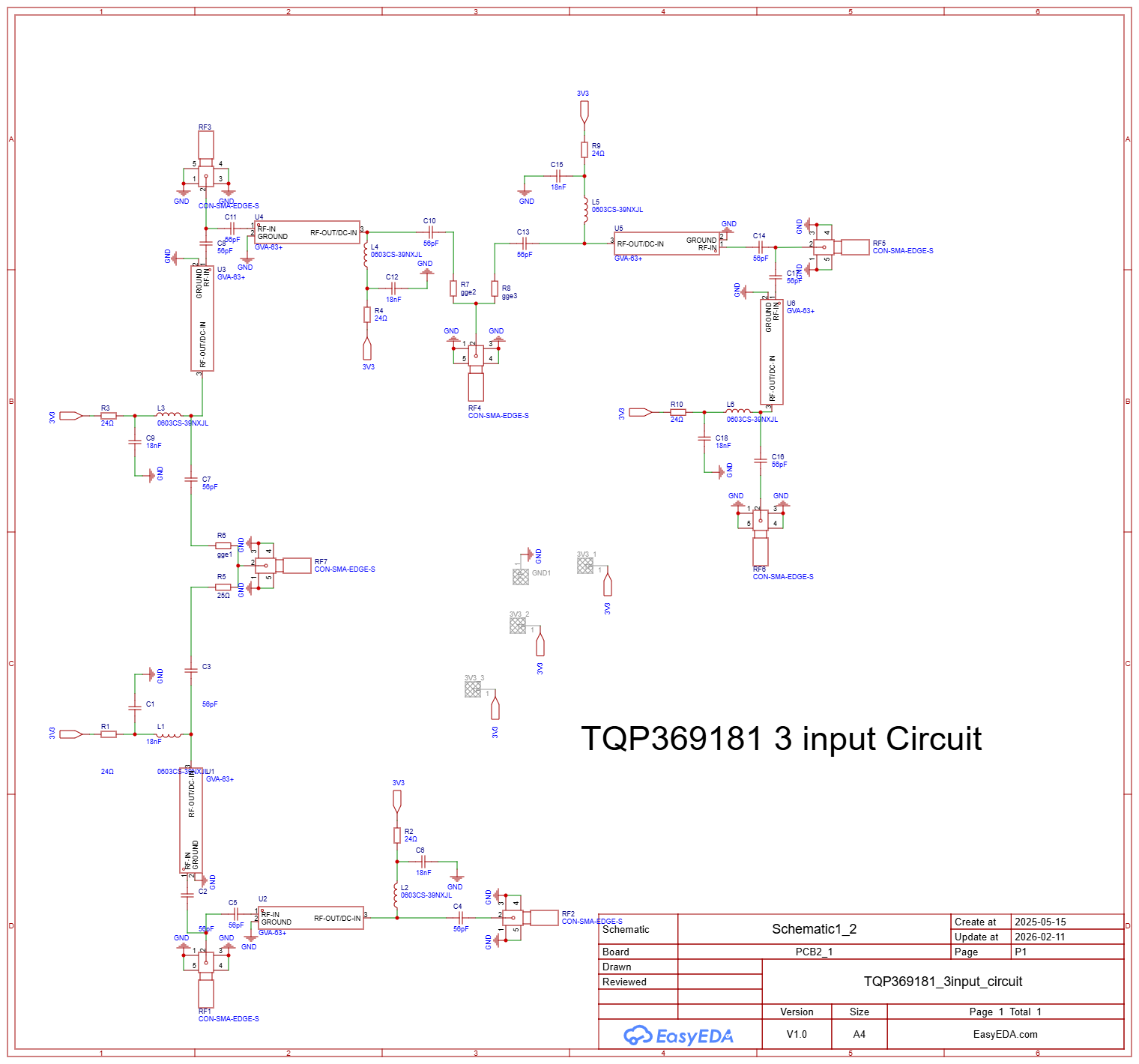
- Six gain stages: GVA-63+ wideband MMIC amplifiers are arranged in cascaded paths, which gives much more gain than a single stage and suits weak signals.
- Bias tees on every stage: Each amplifier gets its DC power through a 24 Ω resistor and a 39 nH RF choke (0603CS), with an 18 nF bypass capacitor to ground. This keeps DC bias separate from the RF signal.
- DC blocking: 56 pF series capacitors on each input and output isolate the amplifiers from connected equipment.
- Eight SMA connectors: Edge-mount SMA jacks serve as inputs and outputs, and some sit between stages so each part of the chain can be measured or tapped.
- Tuning options: Footprint-only resistor positions (marked as “gge”) are included, so links or attenuators can be fitted between stages during testing.
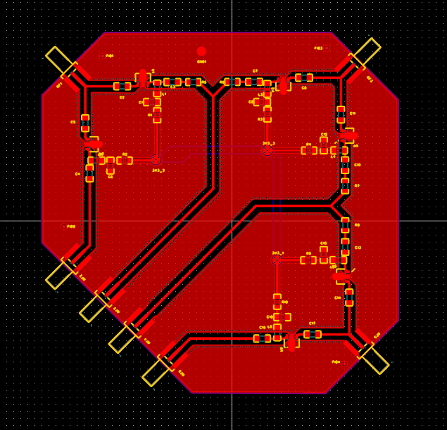
- RF-focused layout: The board is an octagonal shape, with the SMA connectors on the edges and traces routed at 45° angles in 50 Ω lines. The signal paths are surrounded by a solid ground pour with ground via stitching along the traces, which helps isolation between stages and keeps stages from oscillating.
- Assembly aids: Four fiducial marks for machine assembly, and numbered 3.3 V and ground test points.
Design details
Design summary
| CAD tool | EasyEDA |
|---|---|
| Overview | A 50 Ω RF amplifier board that chains several wideband gain stages, with SMA connectors at the inputs, outputs and between stages for measurement. |
| Six gain stages | GVA-63+ wideband MMIC amplifiers are arranged in cascaded paths, which gives much more gain… |
| Bias tees on every stage | Each amplifier gets its DC power through a 24 Ω resistor and a 39 nH RF choke (0603CS), with… |
| DC blocking | 56 pF series capacitors on each input and output isolate the amplifiers from connected… |
| Eight SMA connectors | Edge-mount SMA jacks serve as inputs and outputs, and some sit between stages so each part of… |
| Tuning options | Footprint-only resistor positions (marked as “gge”) are included, so links or attenuators can… |
| RF-focused layout | The board is an octagonal shape, with the SMA connectors on the edges and traces routed at 45°… |
| Assembly aids | Four fiducial marks for machine assembly, and numbered 3.3 V and ground test points. |
Have a board like this?
Send us the schematic, the mechanical constraints and the deadline. We will tell you what it takes and what it costs.