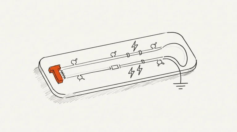
USB 3.0 layout comes down to four rules: 90 ohm differential impedance on the SuperSpeed lane, no more than 150 mils of length mismatch between the pair members, a continuous reference plane directly beneath the pair, and isolation spacing of five times the trace width from neighbouring signals. Miss any one and the board will not open its eye mask, however good the PHY is.
USB is where we see the most preventable failures, because the interface looks easy: two traces, one connector, and the hard work already done in silicon. The decisions that decide whether it works get made in the first hour of layout. Three application notes cover USB layout and they agree on every point that matters.
The impedance target: 90 ohm differential
The number is not a house preference. Microchip’s USB3300 PHY Layout Guidelines states that the USB 2.0 specification requires the DP/DM traces to maintain nominally 90 ohms differential impedance, citing USB specification Rev 2.0, paragraph 7.1.1.3. For SuperSpeed, Texas Instruments’ TUSB73x0 Board Design and Layout Guidelines specifies the pair at 90 ohm plus or minus 15 per cent. 90 ohm is a differential value: it describes the relationship between the two conductors.
Maintain close to 90 Ohms differential impedance. For different dielectric thickness, copper weight or board stack-up, trace width and spacing will need to be recalculated.
That is the practical half of the problem. We do not pick a width from a table and hope. The width comes out of the fabricator’s field solver run against your stack-up, so agreeing the target belongs in the DFM and stack-up review rather than the last hour of layout.
Length matching and total trace length
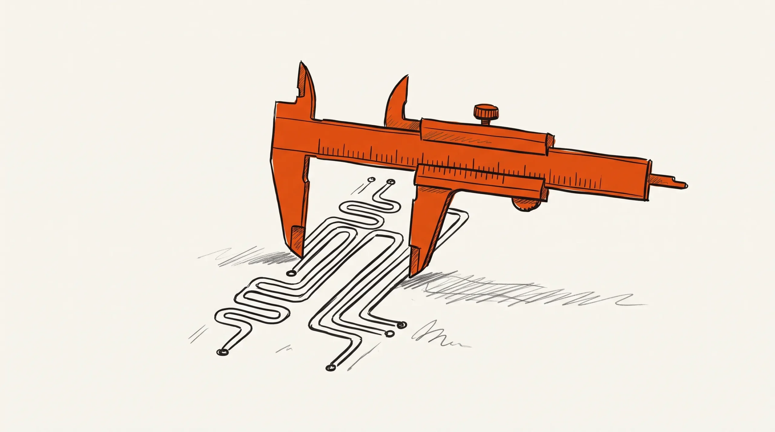
Texas Instruments’ AM335x and AM43xx Sitara Processors USB Layout Guidelines put the mismatch budget plainly: maximum trace-length mismatch between the USB signal pair should not exceed 150 mils. The TUSB73x0 guide gives the same figure for the high-speed pair. The receiver recovers the bit from the difference between the two lines, so a difference in arrival time shrinks that signal. Mismatch is eye height spent on nothing.
Total length is a separate question. TI’s guidance is to keep total trace length to a minimum, and to contact TI if routing longer than eight inches to address signal integrity concerns. Eight inches is where we want a second opinion, not a promise.
There is also an ordering rule in the same document that matters more than it looks. The USB DP and DM signals should be routed as early in the layout process as possible. Once the pair is committed, everything else conforms around it: the plane beneath it, the isolation either side, the vias, the escape at the connector.
The return path, the reference plane and the space around the pair
A differential pair is three conductors. Two traces carry the signal. The third is the reference plane, and it decides whether the two traces work: return current has to get back to the source, and it gets back on the plane directly beneath the pair. The Microchip document requires the ground plane beneath the DP/DM traces, extending at least five times the spacing width to either side.
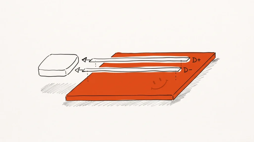
Which is where layer count comes in. TI’s Sitara guidelines note that because of the high frequencies associated with the USB, a printed circuit board with at least four layers is recommended. Four layers is a reference plane decision, not a signal decision. A two-layer board can carry USB if the ground plane stays continuous, but the moment the other side is needed the plane is compromised.
One more rule from the Microchip document, cheap to satisfy and easy to forget: use 45 degree turns rather than a single right angle.
The USB-IF’s USB 3.0 SuperSpeed Equalizer Design Guidelines describe the host compliance test channel as a printed circuit board with eleven inches of trace connecting a standard host connector to SMAs, and state that this eleven inch trace length represents a maximum loss host design comprising PCB plus package. Your board therefore sits inside the loss budget, and the equaliser compensates for loss your own artwork contributes. That is what our high-speed PCB design service is built around.
Isolation and spacing
TI’s Sitara guidelines give the spacing rules directly: route the USB DP and DM signals using the 3W rule, where the traces are separated by three times their width, and isolating DP/DM from other signals by five times the trace width is also highly recommended to minimise crosstalk. These are widely published starting points rather than a guarantee, so check them against what runs alongside the pair.
| Parameter | USB 2.0 pair | USB 3.0 SuperSpeed lane | What to do about it |
|---|---|---|---|
| Differential impedance | 90 ohm nominally, per the USB 2.0 specification | 90 ohm plus or minus 15 per cent | Take width and spacing from the fabricator’s field solver. |
| Max length mismatch | 150 mils between DP and DM | 150 mils between the pair members | Measure the routed pair, not the netlist. |
| Total trace length | No published maximum; keep it minimal | Keep to a minimum. Above eight inches, contact TI | Eight inches is where we ask a question, not a guarantee. |
| Isolation spacing | 3x trace width between pair members, 5x from other signals | Carry the 3x and 5x starting points across | Verify on the artwork, not the schematic. |
| Ground plane | Directly beneath the pair, five times the spacing width to either side | Continuous reference plane; stack-up symmetry is the focus | Keep the plane unbroken for the whole length of the pair. |
| Minimum recommended layer count | At least four layers | At least four layers | A reference plane decision, not a signal decision. |
| Connector type | Type-A or Type-B class receptacle | Type-C, or first-generation Type-A | Take the pin assignment from the connector datasheet. |
What the connector end needs that the controller end does not
The controller end is forgiving. A PHY sits on a quiet board with ground all around it and no competing pins. The connector end is the opposite: the pair starts at a fixed set of pads, on a fixed pitch, in a footprint other pins also need, and everything downstream is measured from there.
- The reference plane cannot break there. The ground plane extending five times the spacing width either side of the pair applies at the connector escape as strictly as anywhere else, and the escape is where footprints are densest.
- Isolation is decided before you draw anything. At a connector, what sits next to the pair is fixed by the pin assignment.
- Length is measured from the connector. The 150 mils mismatch budget and the eight inch total-length question are both referenced to the connector, not the PHY.
A reversible connector such as Type-C adds one more constraint of the same kind: the pair’s exit from the receptacle is set by the receptacle, not by the board, so there is no orientation to choose. Check the pin assignment of the exact part against the connector’s own datasheet before you place it.
The checks to run before release
These are the checks we run before a USB board goes to fabrication. Every one catches something that is expensive later.
- Impedance against the real stack-up. Confirm the field solver returns 90 ohm differential for the stack-up you are building and the width you drew.
- Mismatch on the routed pair. Measure the copper, not the schematic. The budget is 150 mils.
- Total length. Check the pair against the eight inch figure TI asks you to check, and make any longer route a recorded decision.
- Plane continuity. No splits, voids or antipads in the reference plane under the pair, and the plane extending five times the spacing width either side.
- Isolation on the artwork. Three times the trace width between pair members, five times from anything else, measured on the board data.
- Corners and vias. 45 degree turns, no right angles, and the pair’s vias placed as a pair.
- Layer count and stack-up. At least four layers, and a symmetric stack-up.
- The connector end. Pin assignment checked against the connector datasheet, and no right angle at the receptacle.
Running these before release is far cheaper than after a failure. Our PCB design review service exists for this step, the boards we have taken through it are in the project portfolio, and the recurring questions are on the FAQ page.
Frequently asked questions
What impedance should USB 3.0 traces be?
90 ohm differential, with a tolerance of plus or minus 15 per cent for the SuperSpeed lane. The important part is that 90 ohm is a target for your fabricator rather than a width you pick from a table, because the value depends on the stack-up. Dielectric thickness, copper weight and resin content all move it.
How much length mismatch is acceptable?
150 mils maximum between the two members of the pair. Both application notes we use, one for a USB 2.0 PHY and one for a SuperSpeed hub, give the same figure. Mismatch is eye height spent on nothing, so the budget is a difference target rather than a length target, and the two members are matched to each other rather than to a distance.
Is four layers really necessary for USB?
The recommendation is at least four, and the reason is the reference plane rather than the pair. A two-layer board can carry USB if the ground plane stays continuous under the pair, but the moment the other side is needed the plane is compromised. Four layers gives you an unbroken plane, a routing layer and room for the rest of the design.
How is the trace width for 90 ohm worked out?
It is not worked out on its own. You send the fabricator your stack-up and your target impedance, and you get the width and spacing back from their field solver. Dielectric thickness, copper weight and board stack-up all change the answer, so a width right for one stack-up is wrong for another. If the stack-up is still open, close it first.
What is the most common USB layout mistake?
The ground plane under the pair, and the isolation spacing to neighbouring signals. Those two go wrong more often than any impedance or matching error. The plane gets interrupted because something else needed the copper, and the spacing gets squeezed because the pair was routed late into a leftover gap. Both are structural decisions, so they are worth fixing early.
What to send us
If you have a board in front of you, or a schematic about to become one, send us five things: the controller part number, the USB version, the connector type, the target fabricator, and the data rate you intend to run. With those we can tell you the impedance target your fabricator will hit on your stack-up, and whether your layer stack supports the interface.
Routing the board is what the high-speed PCB design service covers, and the fastest way to start is the quote request. If you would rather read the normative text than an application note, the USB-IF document library holds the current specifications and the compliance test specifications.